New Conductor Needed For Nanochips
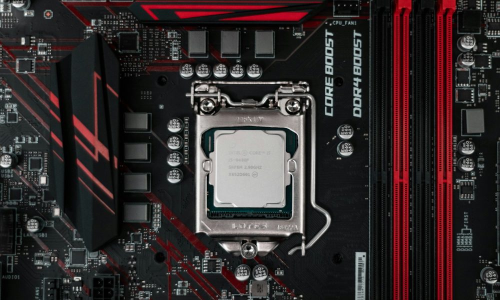
When producing advanced computer chips, the main technological focus has been on reducing the size of transistors and creating more advanced forms of semiconductor materials. This has been the driving force behind the success of companies like TSMC (TSM +4.4%), which are now reaching chip nodes in the 3 or even 2 nm (nanometer) scale.
However, at this scale, some new issues appear that are unrelated to semiconductors. One of them is that traditional conducting materials like copper do not conduct electricity well when the metal wire gets too thin.
This can cause chokepoints for the electricity inside the chips, reducing the computing power and overall efficiency, as well as causing overheating.
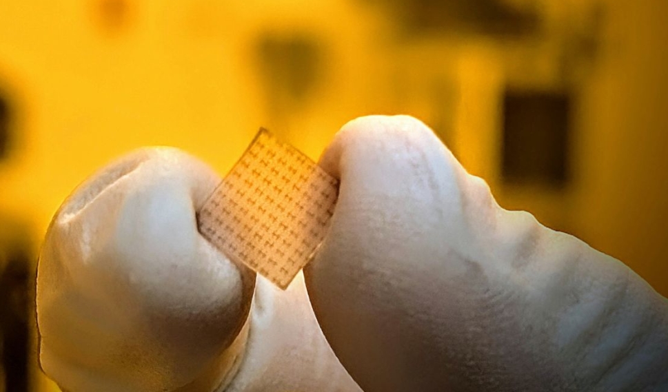
So, it is important news that researchers at Stanford University, Ajou University, Suwon (South Korea), and IBM Watson Research Center have developed an ultrathin material that conducts electricity better than copper in these conditions.
They published their discovery in the prestigious scientific journal Science, titled “Surface conduction and reduced electrical resistivity in ultrathin noncrystalline NbP semimetal”.
Replacing Copper In Computing
Because of its relatively low price and excellent electric conductivity, copper has been the main metal for electric connectivity and is also a key metal in batteries, electric grids, etc.
However, due to copper’s weaker conductivity at nanoscales below 50nm, researchers have been looking for alternatives for a while now. The problem is that known conductors working at the nanoscale level have extremely precise crystalline structures, which need to be formed at very high temperatures.
This could not work for semiconductors and chips, as the high temperature would destroy the fragile silicon components.
So, the race was on to find an ultrathin conductor that did not rely on single-crystalline films.
Niobium Phosphide
The researchers worked with niobium phosphide, a material known to display unique electric properties, like super fast electrons and very high magnetoresistance. It is notably already in use in laser and high-power / high-frequency applications.
Niobium phosphide is called a topological semimetal: this means that while the whole material can carry electricity, the surface is more conductive than the middle.
To simplify the concept a little, we can say the thinner the layer of niobium phosphide, the more surface part there is, with almost no “middle”. As a result, it can be expected that the thinner the niobium phosphide, the more conductive it becomes.
And this is exactly what was observed by the researchers.
“It has been thought that if we want to leverage these topological surfaces, we need nice single-crystalline films that are really hard to deposit. Now we have another class of materials – these topological semimetals – that could potentially act as a way to reduce energy usage in electronics.”
Akash Ramdas – a doctoral student at Stanford
This is a very new field, with physicists having started to experiment with topological semimetals only since 2015. And
Lower Temperature For Computing Applications
The lower temperature means the niobium phosphide is somewhat disorganized, with only nanocrystals in an amorphous matrix.
Source: Stanford Report
Upon further analysis, it appears that the high conductivity is driven by conductive channels at the surface of the ultrathin film.
The film can be deposited at only 400°C (752°F), a temperature low enough to not damage the nearby silicon transistors in a computer chip. So this would make it an ideal material for connecting the internal component of a chip with low resistance and, therefore, low heat production.
“If you have to make perfect crystalline wires, that’s not going to work for nanoelectronics.
But if you can make them amorphous or slightly disordered and they still give you the properties you need, that opens the door to potential real-world applications.”
Yuri Suzuki – Professor of Applied Physics
High Conductivity
When compared to normal films of niobium phosphide, the 5nm thin film was 6x more conductive. This was also lower than usual metals like copper.
When 1.5 nm thin, the material was twice as conductive as copper.
So, this is truly the very first example of non-crystalline, low-temperature conductors that outperform normal metals’ conductivity at the nanoscale.

Source: Stanford Report
“Really high-density electronics need very thin metal connections, and if those metals are not conducting well, they are losing a lot of power and energy.
Better materials could help us spend less energy in small wires and more energy actually doing computation.”
Eric Pop – Professor of Electrical Engineering
The Next Steps
The very next step is to test in a real chip how well niobium phosphide wire works when applied to nanoelectronics, not only for conductivity but also for reliability and how it can be integrated into the manufacturing process.
For that, they will first need to build at-scale niobium phosphide nanowire.
Another work will be to check if this concept could not be better carried by other semimetals that might work even better than niobium.
“For this class of materials to be adopted in future electronics, we need them to be even better conductors. To that end, we are exploring alternative topological semimetals.”
Xiangjin Wu, a doctoral student at Stanford
Heat removal is now one of the main power-consuming processes in these data centers, as much as the computing itself. This is especially true for 5-3 nm chips, required for AI training and the most complex calculations.
So, in the long run, materials conductive at the nanoscale will be a must, as heat production is becoming an increasingly large problem for data centers using advanced chips.
It is also possible that ultrathin niobium phosphide films will find other applications in advanced technologies, especially where this material is already used like laser or telecom equipment.
Investing In Advanced Conducting Materials
As advanced chips and semiconductors elements get smaller, the industry is concentrating toward a handful of large manufacturers like TSMC (TSM +4.4%), Intel (INTC +0.05%) or Nvidia (NVDA -1.28%) (follow the links for dedicated reports for each of these companies).
You can invest in semiconductor-related companies through many brokers, and you can find here, on securities.io, our recommendations for the best brokers in the USA, Canada, Australia, the UK, as well as many other countries.
Or, if you prefer a more diversified approach, you can invest in semiconductor-related ETFs like the iShares Semiconductor ETF (SOXX), the VanEck Semiconductor ETF (SMH), or the Global X Semiconductor ETF (SEMI).
You can also learn more about the semiconductor manufacturing equipment supply chain and key companies in “Top 10 Semiconductor Equipment Stocks for Manufacturing Support”.
Computing Advanced Material Company
International Business Machines Corporation
International Business Machines Corporation (IBM +0.11%)
International Business Machines Corporation (IBM) was the leading force behind the commercialization of the first mainframe computer. It was also the main industrial partner with the Stanford researchers for their niobium phosphide project.
The company has fallen behind in the production volume of other tech giants like Apple, TSMC, and NVIDIA.
It is, however, at the forefront of the development of new computing materials and technology.
IBM is at the forefront of progress in conducting technology, and topological semimetals are just one of those fields. So it is not only ahead in new ultrathin conducting material, but also in high-temperature superconductors.
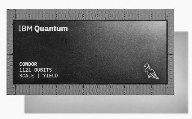
Such superconductors are crucial for quantum computers. Recently, IBM developed “Condor”, a 1,121 superconducting qubit quantum processor based on cross-resonance gate technology, together with “Heron”, a quantum processor at the very edge of the field.

Source: IBM
IBM is involved in most of the other cutting-edge innovations in computing and the semiconductors industry. These include conducting organic materials, neuromorphic computing, photonics, etc.

Source: IBM
To some extent, IBM has become a “patent company” with expertise in developing new computing methods and licensing them to the industry.
So far, IBM seems very determined to hold as many key patents in all the non-silicon computing methods as it can get, replicating its past success when contributing massively to developing the semiconductor industry into the giant it is today.
Niobium phosphide and other topological semimetals-related technologies would fit right in that strategy, with IBM developing the technology to replace copper in these cases, and then licensing it out to the large chip foundries for the manufacturing steps.
